Quantcast
Channel: Forums - Recent Threads
Viewing all 262198 articles
Browse latest View live

TMS320F28379D: EXTSYNCIN1 Trigger Edge

$
0
0

Part Number:TMS320F28379D

Hi,

I need to do inter-boards isolated PWM synchronization and synchronize as precisely as possible all the DSPs PWM together on all boards.

The technical reference manual and the datasheet shows that the EXTSYNCOUT is stretched 8 PLLSYSCLK cycles. The datasheet specify the minimum number of cycles for SYNCIN in asynchronous, synchronous and with input qualifier.

The technical reference manual specify the delay from a master ePWM module to a slave ePWM module in TBCLK and EPWMCLK cycles. The technical reference manual depicts ePWM SYNC in the ePWM module time-base waveforms or in its different sub-modules diagrams as being active on the rising edge. These diagrams are functional diagrams, not timing diagrams.

There is no detailed timing diagram for the SYNCIN inputs in the datasheet. :(

There is also no maximum width specified for SYNCIN in the datasheet (obviously needs to be far less than the PWM period itself). Question in original thread was about the trigger edge. I don't know what is the exact meaning of "The synchronization is fixed as active low." in the original thread answer. I need an answer based on the real behavior of the ePWM sync input internally.

If my inter-boards isolated synchronization mechanism is extending the synchronization pulse to a value greater than 8 PLLSYSCLK or if I use any other global synchronization pulse method to send it to all boards at once, how the ePWM modules will align to this pulse (i.e. give detailed timing diagram)?

Is it only edge aligned to the rising edge of the external synchronization pulse (plus some minimal sampling delay like 1 or 2 EPMWCLK if asynchronous in input qualifier) and a long external synchronization pulse will generate one and only one internal synchronization pulse for each external pulses received (as depicted in the functional diagrams in the technical reference manual)?

Thanks

P.S. A short mention in the datasheet about the real internal alignment in ePWM module near the SYNCIN pulse requirement would resolve all this.

RE: ADS127L01EVM: Output waveform

$
0
0

Hi Ryan.

I collected data with decimal number and got that results what does this mean?

I expect results shown like diagram. What should I do


AWR1642BOOST: Connecting and controlling to mmWave Studeo via USB

$
0
0

Part Number:AWR1642BOOST

Hi, I purchased the AWR1642BOOST auto radar evaluation board to do some basic tests with some measurement equipment.  I'm not a programmer, so I would like to have a simple GUI to allow me to control all the characteristics of the FMCW chirp.  From what I can tell, the correct tool is mmWave Studio.  It definitely has all the controls I'm looking for, but I can't get it to connect to my eval board.  When I plug it into the USB on my PC, I can see the two COM ports (8 and 9 in my case) and I'm able to connect to the board using mmWave Demo Visualizer, so I'm pretty sure the drives are installed and up to date.

In the mmWave Studio user guide it gives instructions for connecting with a DVA1000 or DevPack.  I'm not sure what those are.  I'm hoping someone can help me get connected and running with just the board that I have. Thanks!

BQ25120A: Delay required from power applied to start of I2C communication?

$
0
0

Part Number:BQ25120A

I've found that if we try to communicate with the BQ25120A before 70 ms after our MCU starts up then the communication fails.  I don't see anything in the data sheet about this.  Is this specified somewhere? If not are the min/typ/max values available elsewhere?

BQ24773: BQ24773 IADP PIN and IBAT pin Voltage issue

$
0
0

Part Number:BQ24773

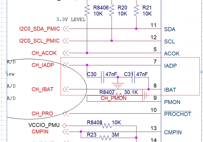
Hi,now my customer uses BQ24773 for charger,now above question need you help to check it,tks!

11pin:SDA 、12pin:SCL、 5pin:ACOK 、10pin:CH_PRO、 13pin:CHPIN、 14pin:CMPOUT; This 6PIN high level is 3.3V, but the 7pin:IADP and  8pin:IBAT  is be connected to the IO of MCU,however,the MCU's IO voltage is 1.8V,but the PIN and IBAT pin  output Voltage is clamped below 3.3 V , now we also recommend LSF0102 to design as 1.8V-3.3V,but in customer view,they want to use Voltage divider resistor to replace the LSF0102,could you help to check it whether is feasible

ADS1262: ADS1262 adc count stability problem

$
0
0

Part Number:ADS1262

Hi

We are using ADS1262  ADC  module for our application.In our application we have the input voltage 1 mV to  2V.

And we are using mV source to test the module .For our test we give the 3mV .when reading the count from ADC module(32 bit) the  nearly 1000000 counts were jumped from mean value.and also i tested the adc count by truncating last 8 bits and 16 bits.

Please help me in this issue and how to stabilize the ADC count, and we have bought 50 nos module for our production.so please consider this as critical issue.

we are configured the module by default module settings and PGA  - 32V.

the results given below and attached the graph also

the count value jump from mean value.the readings are given below

3mv --- count is  87475544   (for 32 bit count ),

highest count  from mean value  -  88201325

Lowest count  from  men value    -  86626213

1575112  counts jumping from lowest to highest.

3mv --- count is  340791   (for 32 bit count  last LSB were truncated ( adc_count >> 8),

highest count  from mean value  -   343045

Lowest count  from  men value    -  336827 

6000 counts jumping from lowest to highest.

3mV --- count is    1349  (  (for 32 bit count  16bits were truncated ( adc_count >> 16)

highest count  from mean value    -   1357

Lowest count  from  mean value    -  1338 

nearly 19  counts jumping from lowest to highest.

88201325

RTOS/CC3220SF-LAUNCHXL: CC32xx P2P Application Source Code or Project Files

$
0
0

Part Number:CC3220SF-LAUNCHXL

Tool/software: TI-RTOS

Hello:

I am in search of the actual project or source code to the CC32xx P2P application.

When I do an online search, the only thing that comes up is the TI wifi wiki - in this wiki, it explains how to run the project but there isn't an associated project or source files.

I also did a search through my installed SDK and cannot find anything.

Can someone help me out?

CCS/MSP430FR5994: ADC12 minimum voltage detection or detecting shut off voltage

$
0
0

Part Number:MSP430FR5994

Tool/software: Code Composer Studio

Hi, I've been trying to store the system clock cycle just before it shuts off in FRAM

to do that I've been using the adc12 windows comparater

for the high voltage threshold i set it to 2.3 and the low threshold to 1.9

but the low threshold interrupt never goes off when it is 1.9 or even 2 it works fine if the threshold is at around 2.1 

I'm wondering what is the minimum voltage detection of the ADC12 and if its not as low as 1.9 or 1.8 which i suspect, what else can i use to detect a low voltage such as 1.8 to 1.9

Thanks for any help and the code that i used is posted below 

void initAdcMonitor()
{
    /* Initialize timer for ADC trigger. */
    TA0CCR0 = (SMCLK_FREQUENCY/ADC_MONITOR_FREQUENCY);
    TA0CCR1 = TA0CCR0/2;
    TA0CCTL1 = OUTMOD_3;
    TA0CTL = TASSEL__SMCLK | MC__UP;

    /* Configure internal 2.0V reference. */
    while(REFCTL0 & REFGENBUSY);
    REFCTL0 |= REFVSEL_1 | REFON;
    while(!(REFCTL0 & REFGENRDY));

    ADC12CTL0 = ADC12SHT0_2 | ADC12ON;
    ADC12CTL1 = ADC12SHS_1 | ADC12SSEL_0 | ADC12CONSEQ_2 | ADC12SHP;
    ADC12CTL3 = ADC12BATMAP;
    ADC12MCTL0 = ADC12INCH_31 | ADC12VRSEL_1 | ADC12WINC;
    ADC12HI = (uint16_t)(4096*((ADC_MONITOR_THRESHOLD+0.4)/2)/(2.0));
    ADC12LO = (uint16_t)(4096*(ADC_MONITOR_THRESHOLD/2)/(2.0));
    ADC12IFGR2 &= ~(ADC12HIIFG | ADC12LOIFG | ADC12INIFG);
    ADC12IER2 = ADC12INIE;
    ADC12CTL0 |= ADC12ENC;
}
#pragma vector = ADC12_VECTOR
__interrupt void ADC12_ISR(void)
{
    switch(__even_in_range(ADC12IV, ADC12IV_ADC12LOIFG)) {
        case ADC12IV_NONE:        break;        // Vector  0: No interrupt
        case ADC12IV_ADC12OVIFG:  break;        // Vector  2: ADC12MEMx Overflow
        case ADC12IV_ADC12TOVIFG: break;        // Vector  4: Conversion time overflow
        case ADC12IV_ADC12HIIFG:                // Vector  6: Window comparator high side
            /* Disable the high side and enable the low side interrupt. */
            break;
        case ADC12IV_ADC12INIFG:

            check = 0;
            ADC12IER2 &= ~ADC12INIE;
            ADC12IER2 |= ADC12LOIE;
            ADC12IFGR2 &= ~ADC12LOIFG;
            break;
        case ADC12IV_ADC12LOIFG:                // Vector  8: Window comparator low side
            //P1OUT |= BIT1;
            P1OUT &=~ BIT0;
            //P1OUT |= BIT0;
            count = count+1;
            status = nvs_data_commit(nvsHandle4, &count);
            /* Disable the low side and enable the high side interrupt. */
            ADC12IER2 &= ~ADC12LOIE;
            ADC12IER2 |= ADC12INIE;
            ADC12IFGR2 &= ~ ADC12INIFG;
            break;
        default: break;
    }
}


DP83TC811R-Q1: schematic review

$
0
0

Part Number:DP83TC811R-Q1

Hi,

Could you help review the schematic of dp83tc811?

1. The customer would like to do MII and RMII compatible design, is that ok? For unused MAC interface pins, can we leave it to float?

2. Why need CM termination/MDI coupling and ESD shunt circuit? How does it work? Can I remove the ESD protection?

Thanks

Dongbao

LAUNCHXL-F28377S: ePWM Pins are HIGH at startup

$
0
0

Part Number:LAUNCHXL-F28377S

Hello,

I am driving a full bridge with the Delfino Launchpad board. I am using the ePWM pins (ePWM6A and ePWM6B) as the low and high side inputs for an arm, and they are at high state for a short moment when the board is energized. In fact, as I am pushing the reset button, those pins are always high. This results in overshoot of course. When the power cables are connected, my power supply disables the output because of the current limit when the overshoot occurs, and the processor is reset because of low voltage on power supply so the pins go high again, and overshoot occurs again and the processor is reset, this goes on like this. As a result, the processor never gets stabilized and gets locked up in a bad state.

I was wondering if this is an issue with Delfino, or just I have to use some additional logic (some logic gates on an additional board) in order to prevent high and low side inputs going high at the same moment?

Thanks,

RTOS/TDA2PXEVM: Assertion at CIO while running the use case

$
0
0

Part Number:TDA2PXEVM

Tool/software: TI-RTOS

Hello 

We are using TDA2PX evm with PSDK3.03 sysbios all configuration. While running the binaries using CCS we are getting assertion with following logs on CCS Console.

IPU1-1 Remote Log Shared Memory @ 0xbfc2e8a0
HOST Remote Log Shared Memory @ 0xbfc310a0
DSP1 Remote Log Shared Memory @ 0xbfc360a0
DSP2 Remote Log Shared Memory @ 0xbfc388a0
EVE1 Remote Log Shared Memory @ 0xbfc3b0a0
EVE2 Remote Log Shared Memory @ 0xbfc3d8a0
EVE3 Remote Log Shared Memory @ 0xbfc400a0
EVE4 Remote Log Shared Memory @ 0xbfc428a0
IPU2 Remote Log Shared Memory @ 0xbfc450a0
Assertion @ Line: 216 in utils_cio.c: gpfid!=NULL : failed !!!
[C66xx_DSP1] Assertion @ Line: 216 in utils_cio.c: gpfid!=NULL : failed !!!
[ARP32_EVE_1] Assertion @ Line: 216 in utils_cio.c: gpfid!=NULL : failed !!!
[Cortex_M4_IPU1_C1] Assertion @ Line: 216 in utils_cio.c: gpfid!=NULL : failed !!!
[C66xx_DSP2] Assertion @ Line: 216 in utils_cio.c: gpfid!=NULL : failed !!!
[ARP32_EVE_2] Assertion @ Line: 216 in utils_cio.c: gpfid!=NULL : failed !!!

If we try to make appimage from the same binaries and try to boot in SD card, it stops after loading appimage from SD card.


This error comes randomly . Will you please let us know how to resolve this error.

regards

Hrishikesh

IWR1642BOOST: Detected points on Demo Visualizer

$
0
0

Part Number:IWR1642BOOST

A simple questione about detected points on Demo Visualizer: are they sent by the board on the DATA_port or are they calculated directly by the program of Demo Visulizer?

Thanks.

Regards.

TPS7A39: DSC LAND PATTERN DATA

$
0
0

Part Number:TPS7A39

I am trying to create a land pattern for this part based on your Land Pattern Example (page 49) of your revised datasheet dated September 2017.

I see that Texas Instruments' land pattern is now based on SOLDER MASK DEFINED pads.  Is this recommended by Texas Instruments?

When I create parts in my library, I always make my pads NON-SOLDER MASK DEFINED.

TPS65983: TPS65983EVM configure problem

$
0
0

Part Number:TPS65983

HI,

I bought a TPS65983EVM from TI store, I have some questions:

I set the board to emulate as a mid power charger adapter(CFG ID#12). I want to change the source PDO from 12V/3A to 12V/2A.

Just only change the maximum current.

Can you send me the tool to modify it?

or Can you modify the code, and then send me the new binary file or hex file.

thanks.

DRV8812: VMX voltage ripple

$
0
0

Part Number:DRV8812

HI, Team:

Do we have some power supply ripple requirement on the VMx pin?

My customer found when the motor running, the ripple on VMx pin is about 1Vpp, and not sure if the chip can accept or not.

Thanks!


CCS/LAUNCHXL-F28379D: CCS/LAUNCHXL-F28379D:

$
0
0

Part Number:LAUNCHXL-F28379D

Tool/software: Code Composer Studio

Hello, I am trying SPI Communication, when I set clock frequency SpiaRegs.SPIBRR.all =0x007F; and clock frequency for SPI should be LSPCLK (50Mhz)/128=390KHz but I am reading from oscilloscope half of it, 195 Khz. Why does it happen? I am missing any other configuration? 

Thanks,

Omer


CCS/MSP432P401R: Error re-programming example program

$
0
0

Part Number:MSP432P401R

Tool/software: Code Composer Studio

I just got a new MSP432401R launchpad. It asked to update the XDS110 the first time I programmed it, so I assume that it is up to date.

I can re-program the gpio_toggle_output example just fine. But when I run the timer_32periodic_mode_led_toggle example (code below), it programs fine the first time, but any subsequent re-programs give me the following error:

CS_DAP_0: Error connecting to the target: (Error -614 @ 0x0) The target indicates there is an error condition from a previous SWD  request.
Clear the error the condition, and try the SWD request again. (Emulation package 7.0.188.0)

And I can only cancel. Once I pull the USB and put it back in, everything is fine.

I thought it might be the fact that it is in LPM0 mode, so I commented that out of the while loop, but still had the same problem. Any thoughts?

/*******************************************************************************
 * MSP432 Timer32 - Periodic LED Blink
 *
 * Description: Starts timer on a button press, toggles GPIO/LED for
 * a timer period, and then turns off LED at end of period.
 *
 *                MSP432P401
 *             ------------------
 *         /|\|                  |
 *          | |                  |
 *          --|RST         P1.1  |<--- Switch
 *            |                  |
 *            |                  |
 *            |            P1.0  |---> LED
 *            |                  |
 *            |                  |
 *
  *******************************************************************************/
/* DriverLib Includes */
#include <ti/devices/msp432p4xx/driverlib/driverlib.h>

/* Standard Includes */
#include <stdint.h>
#include <stdbool.h>

int main(void)
{
    /* Halting the Watchdog */
    MAP_WDT_A_holdTimer();

    /* Setting MCLK to REFO at 128Khz for LF mode */
    MAP_CS_setReferenceOscillatorFrequency(CS_REFO_128KHZ);
    MAP_CS_initClockSignal(CS_MCLK, CS_REFOCLK_SELECT, CS_CLOCK_DIVIDER_1);
    MAP_PCM_setPowerState(PCM_AM_LF_VCORE0);

    /* Configuring GPIO */
    MAP_GPIO_setAsOutputPin(GPIO_PORT_P1, GPIO_PIN0);
    MAP_GPIO_setOutputLowOnPin(GPIO_PORT_P1, GPIO_PIN0);
    MAP_GPIO_setAsInputPinWithPullUpResistor(GPIO_PORT_P1, GPIO_PIN1);
    MAP_GPIO_clearInterruptFlag(GPIO_PORT_P1, GPIO_PIN1);
    MAP_GPIO_enableInterrupt(GPIO_PORT_P1, GPIO_PIN1);

    /* Configuring Timer32 to 128000 (1s) of MCLK in periodic mode */
    MAP_Timer32_initModule(TIMER32_BASE, TIMER32_PRESCALER_1, TIMER32_32BIT,
            TIMER32_PERIODIC_MODE);

    /* Enabling interrupts */
    MAP_Interrupt_enableInterrupt(INT_PORT1);
    MAP_Interrupt_enableInterrupt(INT_T32_INT1);
    MAP_Interrupt_enableMaster();

    /* Sleeping when not in use */
    while (1)
    {
        MAP_PCM_gotoLPM0();
    }
}

/* GPIO ISR */
void PORT1_IRQHandler(void)
{
    uint32_t status = MAP_GPIO_getEnabledInterruptStatus(GPIO_PORT_P1);
    MAP_GPIO_clearInterruptFlag(GPIO_PORT_P1,status);

    if (GPIO_PIN1 & status)
    {
        MAP_GPIO_disableInterrupt(GPIO_PORT_P1, GPIO_PIN1);
        MAP_GPIO_setOutputHighOnPin(GPIO_PORT_P1, GPIO_PIN0);
        MAP_Timer32_setCount(TIMER32_BASE,64000);
        MAP_Timer32_enableInterrupt(TIMER32_BASE);
        MAP_Timer32_startTimer(TIMER32_BASE, true);
    }
}

/* Timer32 ISR */
void T32_INT1_IRQHandler(void)
{
    MAP_Timer32_clearInterruptFlag(TIMER32_BASE);
    MAP_GPIO_setOutputLowOnPin(GPIO_PORT_P1, GPIO_PIN0);
    MAP_GPIO_enableInterrupt(GPIO_PORT_P1, GPIO_PIN1);
}
/******************************************************************************* * MSP432 GPIO - Toggle Output High/Low * * Description: In this very simple example, the LED on P1.0 is configured as * an output using DriverLib's GPIO APIs. An infinite loop is then started * which will continuously toggle the GPIO and effectively blink the LED. * * MSP432P401 * ------------------ * /|\| | * | | | * --|RST P1.0 |---> P1.0 LED * | | * | | * | | * | | * ******************************************************************************/ /* DriverLib Includes */ #include <ti/devices/msp432p4xx/driverlib/driverlib.h> /* Standard Includes */ #include <stdint.h> #include <stdbool.h> //![Simple GPIO Config] int main(void) { volatile uint32_t ii; /* Halting the Watchdog */ MAP_WDT_A_holdTimer(); /* Configuring P1.0 as output */ MAP_GPIO_setAsOutputPin(GPIO_PORT_P1, GPIO_PIN0); while (1) { /* Delay Loop */ for(ii=0;ii<50000;ii++) { } MAP_GPIO_toggleOutputOnPin(GPIO_PORT_P1, GPIO_PIN0); } } //![Simple GPIO Config]

UCC28730: PMP40025 Reference design vs UCC28730

$
0
0

Part Number:UCC28730

Hello,

I am designing an isolated 48V, 1A AC-DC Converter using UCC28730 based on PMP40025  Reference design.

In the reference design 48V is generated using UCC28730  but when I try to do same on webench design, It shows the maximum output voltage as 22V. 

Why is this? Is the reference design right or the webench?

Regards

Vishal Kakade

SN65DSI85: Schematic review request

$
0
0

Part Number:SN65DSI85

Can I email someone at TI my schematic for a quick review.  We've used the SN65DSI83 successfully I just want to do double check this SN65DSI85 design.

Thank you

AM5728: Baud rate differs between UART's

$
0
0

Part Number:AM5728

Hi,

Both UART1 and UART3 are using the FUNC_48M_CLK.  I am using 0x1a in the baud rate low byte, 0 in the high byte.

UART3 has a bit time of around 8.6 usec, this translates to around 115k baud.  UART1 on the other hand has a bit time of around 8.8 translating to around 113k baud. 

The serial port receiving this data is tolerant of the 115k baud but is not able to handle data at 113k baud.

Why are the two UARTs demonstrating different bit times with the exact same settings?

Thanks

Kevin

Viewing all 262198 articles
Browse latest View live


<script src="https://jsc.adskeeper.com/r/s/rssing.com.1596347.js" async> </script>