↧
BQ2004: 15cells application
↧
TLV5630: TLV5630 12 bit
Part Number:TLV5630
Hello All,
I am trying to send some data from Tms320f28335 dsp to TLV5630 DAC via SPI. I am sending the correct signal to the Dac. I have checked the MOSI, Sclk , FS Pins and they are supposed to act as they should be. Now, I have set var1 ( in code below) from data sheet to obtain my analog data in channel B, but i am getting my data on channel C. Only when i give 0x0000 only then I get actual data on channel A. Otherwise I get right data in wrong channels. Can anyone tell me , what mistake i am making in selecting channels? I am given my initialization and my methodology below.
daco = (vref*5); // some sinusoidal data points
var1 = 0x1000;
sdata1 = var1|daco;
void spi_init()
{
SpiaRegs.SPICCR.all =0x000F; // Reset on, rising edge, 16-bit char bits
SpiaRegs.SPICTL.all =0x0006; // Enable master mode, normal phase,
// enable talk, and SPI int disabled.
SpiaRegs.SPIBRR =0x0014;
SpiaRegs.SPICCR.all =0x009F; // Relinquish SPI from Reset
SpiaRegs.SPIPRI.bit.FREE = 1; // Set so breakpoints don't disturb xmission
}
void spi_fifo_init()
{
// Initialize SPI FIFO registers
SpiaRegs.SPIFFTX.all=0xE040;
SpiaRegs.SPIFFRX.all=0x204f;
SpiaRegs.SPIFFCT.all=0x0;
}
void spi_xmit1(Uint16 a)
{
SpiaRegs.SPITXBUF=a;
l1=1;
l1=2;
l2=l1/2;
GpioDataRegs.GPASET.bit.GPIO30 = 1;
l2=1;
l2=2;
GpioDataRegs.GPACLEAR.bit.GPIO30 = 1;
}
↧
↧
ADS1292RECG-FE: ADS1292RECG-FE
Part Number:ADS1292RECG-FE
Dear Sir/Madam,
I cannot seem to find a Windows-10 USB driver for the ADS1292R interface eval board. Can you assist?
If there is an alternative method of interrogating the ADS1292R please advise also.
Regards,
Jean Orhan
↧
CC-ANTENNA-DK2: I am looking for the shop which we can buy MXJA01JA1200
Part Number:CC-ANTENNA-DK2
Hi TI Experts,
Please let me confirm the following question.
[Question]
I would like to buy the uSMA-uSMA cable "MXJA01JA1200" in Antenna-DK2. Where can we buy it?
Best regards.
Kaka
↧
INA270A-Q1: the Max Full Range Offset +- 3mV is applied at the fixed Gain = 14 ?
Part Number:INA270A-Q1
Hi Team
may I get your quick response ?
INA270A-Q1 has Max Full Range Offset = +- 3mV and Gain = 14[V/V].
customer wants to know the max offset at the fixed Gain = 14[V/V].
the Max +- 3mV offset is applied at Gain = 14[V/V] ?
or I has to calculate Max +- 42mV offset by (3mV x 14) ?
I believe INA270(Gain 14) and INA271(Gain 20) have the fixed gain respectively,
so that the Max full range offset is applied at the fixed gain,
but I need BU's confirm.
↧
↧
TMS320DM368: PU/PD of YOUT[7:0] when not use them
Part Number:TMS320DM368
Hello,
My customer is dveloping DM368 but they don't use YOUT[7:0].
Those pins become "Input" when reset and there are no IPU/IPDs.

Should they put PU or PD outside of YOUT[7:0]?
If so, are there recomend value of PU/PD register ?
Regards,
Takeshi Matsuzaki
↧
TPS63050: Inductor Selection @1.0uH or 2.2uH
Part Number:TPS63050
Hi
My Customer has question.
[Table 4. Matrix of Output Capacitor and Inductor Combinations] recommend 1uH, 1.5uH, 2.2uH.
Customer can only use 1 uH or 2.2 uH because of the availability of Inductor.
Is it OK to use 1uH or 2.2uH with the following spec?
I think that either way is OK, but please comment if there are any concerns.
■SPEC
VIN=3.0~3.6V
Vout=3.8V
Iout=0.5A
Cout=20uF
Regard
T Kishi
↧
TCI6638K2K: Errata Clarification:
Part Number:TCI6638K2K
- In “Literature Number: SPRZ401F”, Table 4. Silicon Revision, 3.1 is mentioned as the applicable revision. But in detailed explanation, Revision(s) Affected: 3.1 is not mentioned. Is it a typo and still applicable for 3.1?
- In Usage Note 7, in workaround, it is mentioned that,
- On PG 1.0 silicon, TI recommends that both AVS rails must be tied together.
- On PG 1.1 silicon, these two rails are tied together internally
So, we assume, from 1.1 on wards (even for 2.0,3.0 & 3.1), it’s taken care internally. Please confirm.
↧
TDC7200: Register read write,tof measurement issue
↧
↧
DLP3010: Can I get DLP3010_GUI_Source_code??

↧
Linux/BEAGLEBK: how to configure gpio pins that are not existing??
Part Number:BEAGLEBK
Tool/software: Linux
Hello,
i am working over beagle bone black. i have got a new board for which i have downloaded a new debian image of version 9.3 from beagleboard.org
the image is getting uploaded into my beaglebone.but it has a new gpio directory structure as shown below.
export gpio12 gpio20 gpio3 gpio45 gpio5 gpio65 gpio7 unexport
gpio112 gpio13 gpio22 gpio30 gpio46 gpio50 gpio66 gpiochip0
gpio114 gpio14 gpio23 gpio31 gpio47 gpio51 gpio67 gpiochip32
gpio115 gpio15 gpio26 gpio4 gpio48 gpio60 gpio68 gpiochip64
gpio116 gpio2 gpio27 gpio44 gpio49 gpio61 gpio69 gpiochip96
but my application requires gpio 70 - 80 which are not present in new debian version. my old beaglebone black is of debian versio 7.9 and my old gpio directory structure was
export gpio44 gpio65 gpio70 gpio75 gpio8 gpio88 gpiochip64
gpio10 gpio45 gpio66 gpio71 gpio76 gpio80 gpio89 gpiochip96
gpio11 gpio46 gpio67 gpio72 gpio77 gpio81 gpio9 unexport
gpio23 gpio47 gpio68 gpio73 gpio78 gpio86 gpiochip0
gpio27 gpio61 gpio69 gpio74 gpio79 gpio87 gpiochip32
can anyone please tell me how can i get gpio 70-80
↧
TINA/Spice/UCC28180: Block Modelling

↧
ADS1120: ADS1120 with NodeMCU ESP12E SPI /conversion problem
Part Number:ADS1120
Hello TI Engineering Team,
My company is using ADS1120 communicating with NODEMCU ESP12E (Lolin) over SPI. We are using external precision TI voltage reference of 2.048V. I have attached the schematics as well and code program. When we read the voltage we get accurate reading but in between there are in accurate readings as well. The logic analyzer plot is also attached. Please provide help.
Below are the code snippets and code outputs on serial monitor captures.
#include "SPI.h"
#define cs_pin 15
#define dr_pin 0
byte reg00=0x00;
byte reg01=0x00;
byte reg02=0x00;
byte reg03=0x00;
byte dmsb;
byte dlsb;
byte emsb;
byte elsb;
byte buffer[4];
SPISettings ADS1120(4096000, MSBFIRST, SPI_MODE1);
void setup()
{
// ADS1120 setup
pinMode(cs_pin, OUTPUT); // we use this for CS select pin
pinMode(dr_pin, INPUT); // we use this for DR pin
SPI.begin();
SPI.beginTransaction(ADS1120); // wake up the SPI bus.
// SPI.setBitOrder(MSBFIRST);
// SPI.setDataMode(SPI_MODE1); //CPOL=0, CPHA=1 DO NOT USE HERE VALUE 1 (SPI_MODE1=0x04)!
// Initialize serial communication
Serial.begin(115200);
// wait until the serial stream is not open (Leonardo only)
while (!Serial);
Serial.println("Serial com ready");
// Send RESET command
digitalWrite(cs_pin, LOW);
SPI.transfer(0x06);
digitalWrite(cs_pin, HIGH);
delayMicroseconds(100); // Guard time
// Set up configuration registers
digitalWrite(cs_pin, LOW);
SPI.transfer(0x43); // Write four bytes starting at configuration register 00h
SPI.transfer(0x81); // Register 00h: Read U_MON
SPI.transfer(0x04); // Register 01h: 20SPS, 256KHz modulator clock, Single shot, disable temp sensor, Current sources off
SPI.transfer(0x50); // Register 02h: External Vref, 50Hz rejection, PSW off, IDAC off
SPI.transfer(0x00); // Register 03h: IDAC1 disabled, IDAC2 disabled, dedicated DRDY
digitalWrite(cs_pin, HIGH);
// Read back configuration registers as a sanity check
digitalWrite(cs_pin, LOW);
SPI.transfer(0x23); // Read four bytes starting at configuration register 00h
reg00=SPI.transfer(0);
reg01=SPI.transfer(0);
reg02=SPI.transfer(0);
reg03=SPI.transfer(0);
digitalWrite(cs_pin, HIGH);
Serial.print("Reg00: ");
Serial.println(reg00, HEX); // Display Reg00
Serial.print("Reg01: ");
Serial.println(reg01, HEX); // Display Reg01
Serial.print("Reg02: ");
Serial.println(reg02, HEX); // Display Reg02
Serial.print("Reg03: ");
Serial.println(reg03, HEX); // Display Reg03
}
void loop()
{
if((digitalRead(dr_pin)) == LOW){
digitalWrite(cs_pin, LOW);
//SPI.transfer(0x08); // Start conversion (single shot)
delayMicroseconds(50);
digitalWrite(cs_pin, HIGH);
adc_read();
delay(5000);
}
//SPI.end();
}
void adc_read()
{
digitalWrite(cs_pin, LOW);
SPI.transfer(0x10); // Send RDATA command
delayMicroseconds(50); // Guard time
long Volts = SPI.transfer(0);
Volts = (Volts << 8) | SPI.transfer(0);
float AIN0 = (Volts*2.048)/32767;
Serial.print("AIN0=");
Serial.println(AIN0);
digitalWrite(cs_pin, HIGH);
}
Code Output capture on serial monitor of arduino sketch:
AIN0=1.09
AIN0=0.51
AIN0=1.09
AIN0=2.05
AIN0=1.09
AIN0=1.09
AIN0=1.09
AIN0=4.03
AIN0=1.09
AIN0=1.09
AIN0=1.15
AIN0=1.09
AIN0=1.09
AIN0=3.19
AIN0=3.67
AIN0=1.09
AIN0=1.09
AIN0=1.09
AIN0=1.09
AIN0=4.08
AIN0=1.09
AIN0=1.09
AIN0=1.09
AIN0=1.09
(Please visit the site to view this file)
↧
↧
TDA2EG: Technical Reference Manual
Part Number:TDA2EG
Hi
I am try to find the Technical Reference Manual of TDA2E ( TDA2Ex SoC for Advanced Driver Assistance Systems (ADAS) Silicon Revision 2.0, 1.0 Technical Reference Manual (SPRUI00)? ).
But i can not find it from TI official website, so please tell me where to download the doc, thank you~
Thanks
xuanbo
↧
Linux/AM4378: Error building SDK with X11 using 4.02 SDK source
Part Number:AM4378
Tool/software: Linux
Dear,
We are continuously working on AM4378 based board with sitara linux. Now i want to make java (GUI application) work in sitara linux. Since java is not included in the SDK, I tried to build sdk with X11 from SDK source (4.02.00.09). I referred below web guidelines to build sdk with x11 from sdk source file.

It gives error while building. please find attached terminal error report
.(Please visit the site to view this file)
I run below command to build sdk with X11.
git clone git://arago-project.org/git/projects/oe-layersetup.git tisdk
cd /home/futura/tisdk/
./oe-layertool-setup.sh -f configs/processor-sdk/processor-sdk-04.01.00.06-x11-config.txt
cd build/
. conf/setenv
export PATH=$HOME/gcc-linaro-6.2.1-2016.11-x86_64_arm-linux-gnueabihf/bin:$PATH
MACHINE=am437x-evm bitbake arago-core-tisdk-image
Our ultimate aim is to make java work in sitara linux. I installed utilities like makeinfo,gawk,chrpath, etc.
Kindly provide the way how to make java work in sitara linux?
How do i solve the above attached error while building sdk with X11?
Regards,
Winiston.P
↧
TPS62088: Output filter
Part Number:TPS62088
Hi,
I would like to use an output inductor with 1 μF,
but are there recommended values for output capacitors and other parts?
Best Regards,
Yuto Sakai
↧
TRF372017: RF OUT Frequency range
Part Number:TRF372017
Hi, I am planning to use TRF372017 IQ modulator to generate 4.5 GHz signal from base band I & Q signal.
Does this IC support up to 4.8 GHz signal generation?
LO Frequency range is given 300 MHz to 4.8 GHz. Does it means RF OUT(pin 18) shall be in that range?
In its data sheet i see in one of the typical application Ex, performance of TRF372017 in Table 29, RF OUT range mentioned is 300-4300 MHz!
↧
↧
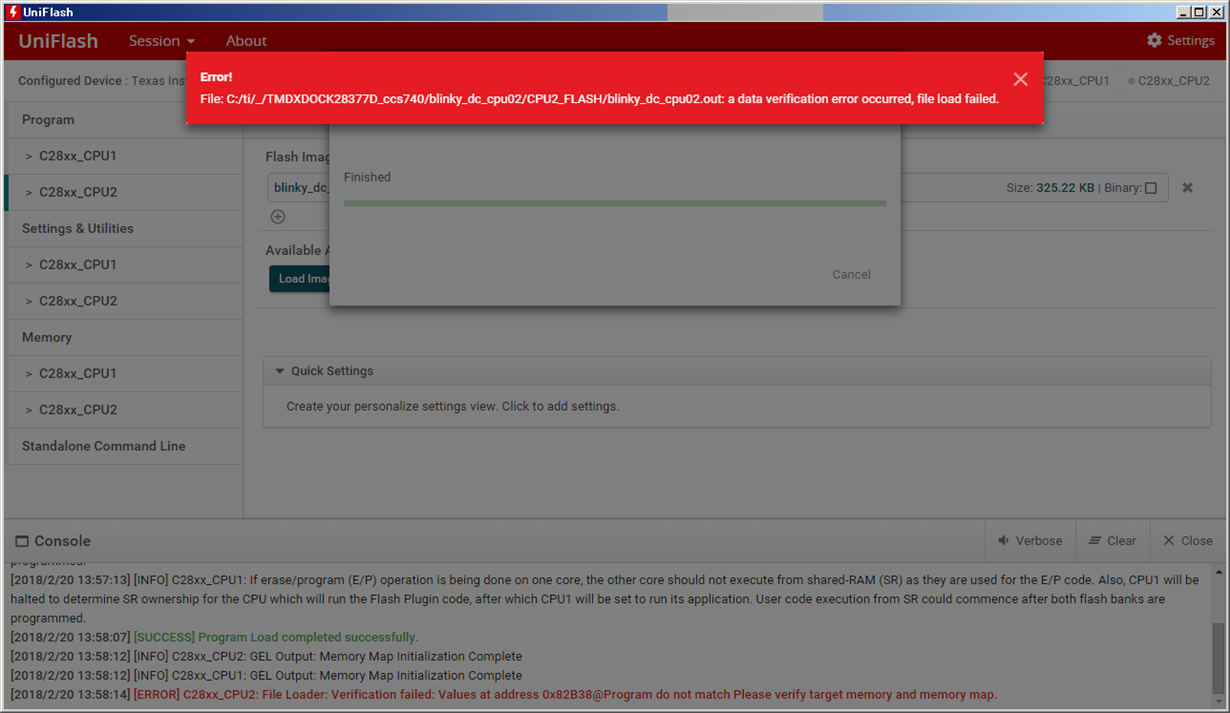
TMS320F28377D: TMS320F28377D: Uniflash422: Settings & Utilities: C28xx_CPU2: Verify Images >>> Error
Part Number:TMS320F28377D
>>
The previous thread:
TMS320F28377D: Uniflash421: Settings & Utilities: C28xx_CPU2: Calculate Checksum >>> Error
e2e.ti.com/.../2367800
<<
Hello,
My Uniflash 4.2.2 console output the following error message. Could you please advise?:
[ERROR] C28xx_CPU2: File Loader: Verification failed: Values at address 0x82B38@Program do not match Please verify target memory and memory map.
Test procedure:
- The source project was blinky_dc_cpu02 in C2000Ware_1_00_03_00.
- The source project was built by CCS740 in build configuration CPU2_FLASH.
- The output blinky_dc_cpu02.out was fed to Uniflash 4.2.2.
- Launch Uniflash 4.2.2.
- Program the blinky_dc_cpu02.out.
- Verify the CPU02 flash. >>> Error.
Findings
- The error points 0x82B38@Program. I attached its map file for reference.
- I also found that the Uniflash memory browser display the address 0x82B38@Program as all 0x0000. (Please be noted that my main point is the verify error.)
- The CPU02 finely blinked when the CPU01 was also porgrammed. Therefore the CPU02 program result should be okay. And the checksum was also okay. So the point would be just verification.
↧
TMS320F28377D: Uniflash422: "Run Target after program load" to remember
Part Number:TMS320F28377D
>>
The previous thread:
TMS320F28377D: Uniflash421: Settings & Utilities: C28xx_CPU2: Calculate Checksum >>> Error.
<<
Hello,
Thank you for your post on 2017/11/23 3:48 AM in the thread above.
Can I ask the status of requesting the "Remember my settings" feature for 'Uncheck'ing the setting for "Run Target after program load" ?
↧
Linux/AM3358: nResetn is asserted low but not deasserting to high again
Part Number:AM3358
Tool/software: Linux
Hello
I have designed a custom board of AM3358 based on the TI AM335x EVM.
The board was booting fine and working fine till yesterday morning.Suddenly it stopped booting and even not responding with CCCCC in the uart . When checked properly its found that the nResetn ouput was asserted low and not becoming high at all.
The nResetn schematic was exactly maintained same as it was in the eval board. i.e. it is used as an output to reset to Ethernet section and connected to jtag .
The pin was pulled high with a pull up resistor.
What would be the problem and what could be the solution for this ?
Kindly reply at the earliest?
Regards
Mad_hu.
↧