Part Number:LAUNCHXL-F28069M
I want to control a CrM (Critical Mode) Boost Circuit. When the inductor current reaches its valley, the ZCD signal gets a rise edge. When the inductor current reaches its peak, the ZCD signal gets a fall edge. The ZCD signal is sent to DSP.
The ZCD connects to the TZ2(GPIO13) pin of DSP,when the rise edge of ZCD is coming,the Digital Compare (DC) Submodule of EPWM2 output the DCAEVT1.sync,as the Figure 3-47 shows. If the time between two rise edge is too small, it can use the Blanking Window to filter the second rise edge of ZCD.

As the Figure 3-5 shows, DCAEVT1.sync can load the TBPHS to TBCTR, then the TBCTR increase from zero. When the TBCTR is cleared, the EPWM2B is set. When the TBCTR equal to CMPB, the EPWM2B is cleared and the EPWM2A is set. When the TBCTR equal to CMPA, the EPWM2A is clear.

There is a ZCD signal input DSP, and then DSP output EPWM2A and EPWM2B, and their relationship is shown in Fig.1.

Fig.1
The reason why I want to use blanking window is that there is interference signal when the inductor current reaches its peak sometimes, as the Fig. 2 shows. The green waveform is my ZCD signal. It seems to be ok. But when you see the light blue waveform, it is the EPWMSYNCO signal, sometimes the light blue waveform get a pluse when the ZCD signal is fall edge. Therefore, I want to use the blanking window to filter the wrong pluse.

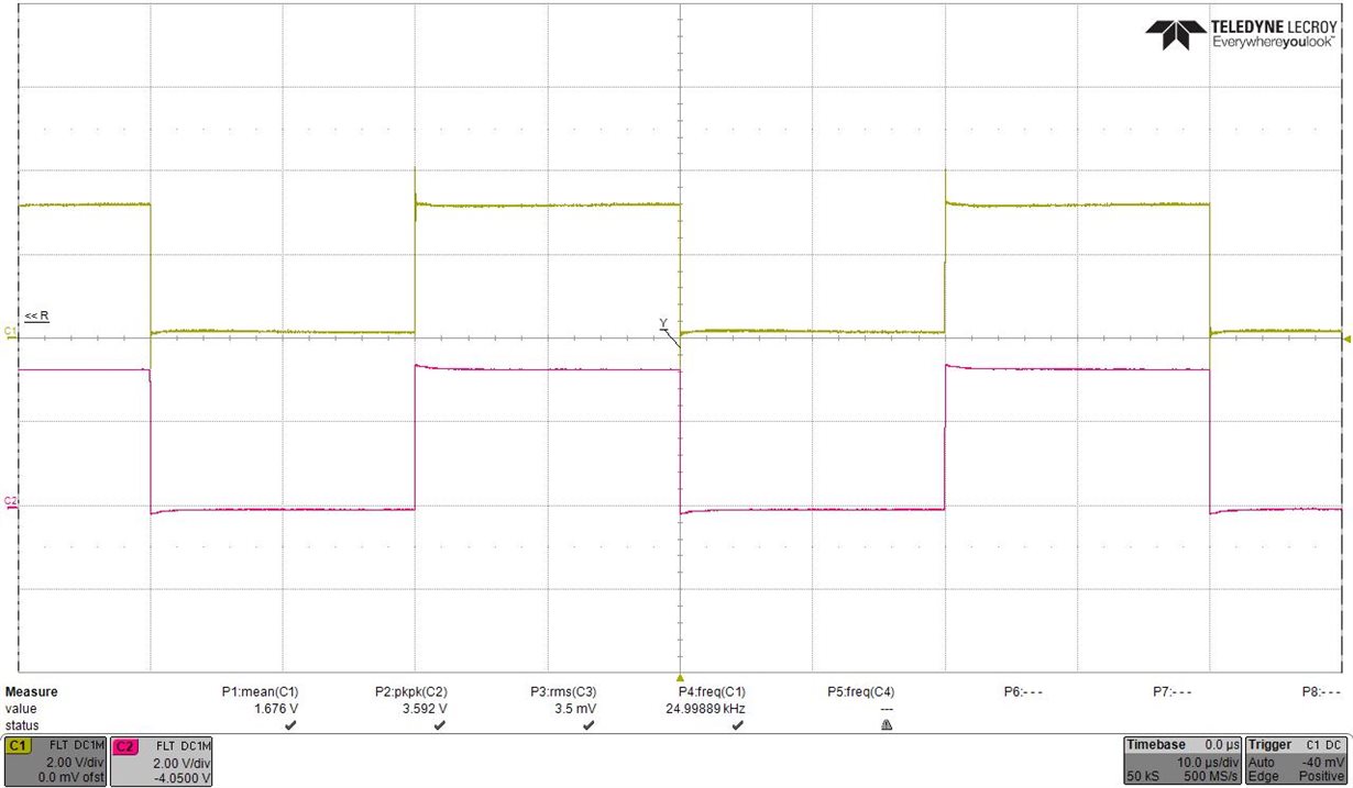
Channel 1: EPWM1B; Channel 2: EPWM1SYNCO; Channel 3: Inductor Current; Channel 4: ZCD signal
Fig. 2
Before I use the code to my Boost circuit. I use the wave generator to generat the ZCD signal and interference signal to verify my code.
As Fig.3 shows, the green waveform is generated by the waveform generator. Its period is 10us. It includes the ZCD signal and the interference signal. The first one rise edge is ZCD signal and the next is interference signal. So the ZCD signal's period is 20us and the interference signal is also 20us. I want the ZCD signal to control the PWM, and the interference signal is ignored by the blanking window. Therefore, my PWM period is 20us. And my OFFSET(9-11us) is smaller than TBPRD(20us).
In my opinion, if the coed is right, the first signal is ZCD signal, then the EPWM1B set high. After 6us, the EPWM1B clear. Then the second signal is interference signal come, it will be filter by blanking window, so the EPWM1B keep zero. But the experimental result do not match.
![]()
Channel 1: EPWM1B; Channel 2:EPWM1A; Channel 4: ZCD signal
Fig.3
There is my code:
#include "math.h"
#include "DSP28x_Project.h"
void InitEPwm2Example(void);
int main(void) {
InitSysCtrl(); // Initialize System Control
InitGpio(); //Initialize GPIO
InitEPwm2Gpio();
InitTzGpio();
//Configure ePWM module
EALLOW;
SysCtrlRegs.PCLKCR0.bit.TBCLKSYNC = 0;
InitEPwm2Example();
SysCtrlRegs.PCLKCR0.bit.TBCLKSYNC = 1;
EDIS;
//wait for timer0 interrupt
for(;;);
}
void InitEPwm2Example(){
// Setup TBCLK
EPwm2Regs.TBCTL.bit.CTRMODE = 0x0; // Count up mode
EPwm2Regs.TBPRD =4500; // Set timer period, for this example set at max value
EPwm2Regs.TBCTL.bit.PHSEN = 0x1; // Enable phase loading
EPwm2Regs.TBPHS.half.TBPHS = 0; // Phase is 0
EPwm2Regs.TBCTR = 0x0000; // Clear counter
EPwm2Regs.TBCTL.bit.HSPCLKDIV = TB_DIV1; // Clock ratio to SYSCLKOUT
EPwm2Regs.TBCTL.bit.CLKDIV = TB_DIV1;
// Setup shadow register load on ZERO
EPwm2Regs.CMPCTL.bit.SHDWAMODE = CC_SHADOW; // Load registers every ZERO
EPwm2Regs.CMPCTL.bit.SHDWBMODE = CC_SHADOW;
EPwm2Regs.CMPCTL.bit.LOADAMODE = CC_CTR_ZERO;
EPwm2Regs.CMPCTL.bit.LOADBMODE = CC_CTR_ZERO;
// Set Compare values
EPwm2Regs.CMPA.half.CMPA = 720; // Set compare A value 8us
EPwm2Regs.CMPB = 450; // Set compare B value 5us
// Set actions
EPwm2Regs.AQCTLA.bit.CBU = AQ_SET; // force EPWM1A output high; the high switch turn on
EPwm2Regs.AQCTLA.bit.CAU = AQ_CLEAR; // force EPWM1A output low; the high switch turn off
EPwm2Regs.AQCTLB.bit.ZRO = AQ_SET; // force EPWM1B output high; the low switch turn on
EPwm2Regs.AQCTLB.bit.CBU = AQ_CLEAR; // force EPWM1B output low; the low switch turn off
//dead time
EPwm2Regs.DBCTL.bit.IN_MODE = 0; // Clear PWM1B on event B, up count
EPwm2Regs.DBCTL.bit.HALFCYCLE = 0; // Clear PWM1B on event B, up count
EPwm2Regs.DBCTL.bit.POLSEL = 0; // Clear PWM1B on event B, up count
EPwm2Regs.DBCTL.bit.OUT_MODE = 2; // Clear PWM1B on event B, up count
EPwm2Regs.DBRED = 9; // Clear PWM1B on event B, up count 0.1us
//DC
EPwm2Regs.DCTRIPSEL.bit.DCAHCOMPSEL = 1; //TZ2 input
EPwm2Regs.TZDCSEL.bit.DCAEVT1 = 2; //DCAH = high, DCAL = don't care
EPwm2Regs.DCACTL.bit.EVT1SYNCE = 1; //SYNC Generation Enabled
EPwm2Regs.DCACTL.bit.EVT1SRCSEL = 0; //0:Source Is DCAEVT1 Signal; 1:Source is DCEVTFILT Signal
EPwm2Regs.TZCTL.bit.DCAEVT1 = 3;
//Filter
EPwm2Regs.DCFCTL.bit.PULSESEL = 1; //Time-base counter equal to zero
EPwm2Regs.DCFCTL.bit.BLANKINV = 0; //Blanking window not inverted
EPwm2Regs.DCFCTL.bit.BLANKE = 1; //Blanking window is enabled
EPwm2Regs.DCFCTL.bit.SRCSEL = 0; //Source is DCAEVT1 Signal
EPwm2Regs.DCFOFFSET = 810; //Blanking Window Offset 9us
EPwm2Regs.DCFWINDOW = 180; //Blanking Window Width 2us
}
Thanks,
Chenkai