Quantcast
Channel: Forums - Recent Threads
Viewing all 262198 articles
Browse latest View live

CC1310: pin_shutdown and I/O interrupt

$
0
0

Part Number: CC1310

I implemented a code to exchange interrupts between two devices like this:


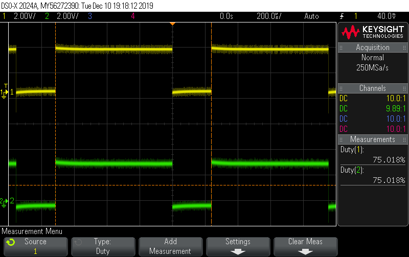
DEVICE 1 I press the button0 and the DEVICE 2 answers me with LED0 on.


Now to this code, I am implementing pin_Shutdown to have a very low consumption after I send it to the command. For the moment I have declared a button that I don't use and the shutdown works.

Can I use the buttons I use to send the command and then send it to shutdown?

I implemented this, but I have problems:

The device sends the command but does not go into shutdown.

PIN_Config ledPinTable[] =
{
	LED_1   | PIN_GPIO_OUTPUT_EN | PIN_GPIO_LOW | PIN_PUSHPULL | PIN_DRVSTR_MAX,
        LED_2   | PIN_GPIO_OUTPUT_EN | PIN_GPIO_LOW | PIN_PUSHPULL | PIN_DRVSTR_MAX,
        BUTTON_0 | PIN_INPUT_EN | PIN_PULLUP | PIN_IRQ_NEGEDGE,	
	PIN_TERMINATE
};

PIN_Config ButtonTableWakeUp[] = {
        BUTTON_0 | PIN_INPUT_EN | PIN_PULLUP | PINCC26XX_WAKEUP_NEGEDGE,
                        
    PIN_TERMINATE                                 /* Terminate list */
};

/* Shutdown Button pin table */
PIN_Config ButtonTableShutdown[] = {
       BUTTON_0| PIN_INPUT_EN | PIN_PULLUP | PIN_IRQ_NEGEDGE,
                          
    PIN_TERMINATE                                 /* Terminate list */
};

static void buttonClockCb(UArg arg) {
    PIN_Handle buttonHandle = (PIN_State *) arg;


    Clock_stop(hButtonClock);


    if (activeButtonPinId != PIN_TERMINATE) {

        if (!PIN_getInputValue(activeButtonPinId)) {

            switch (activeButtonPinId) {
            case BUTTON_0:
                Semaphore_post(Semaphore_handle(&shutdownSem));
                break;
            default:

                break;
            }
        }
    }


    PIN_setConfig(buttonHandle, PIN_BM_IRQ, activeButtonPinId | PIN_IRQ_NEGEDGE);


    activeButtonPinId = PIN_TERMINATE;
}

static void buttonCb(PIN_Handle handle, PIN_Id pinId) {

    activeButtonPinId = pinId;


    PIN_setConfig(handle, PIN_BM_IRQ, activeButtonPinId | PIN_IRQ_DIS);


    Clock_setTimeout(hButtonClock, (50 * (1000 / Clock_tickPeriod)));
    Clock_start(hButtonClock);
}

static void taskFxn(UArg a0, UArg a1)
{

    Semaphore_pend(Semaphore_handle(&shutdownSem), BIOS_WAIT_FOREVER);

    PINCC26XX_setWakeup(ButtonTableWakeUp);

    Semaphore_pend(semHandle, BIOS_WAIT_FOREVER);

    Power_shutdown(0, 0);

    while (1);
}

void Send_Button_Command(PIN_Handle handle, PIN_Id pinId)
{
    CPUdelay(8000*50);
	if (!PIN_getInputValue(pinId))
	{
	  switch(pinId){

	  case BUTTON_0:
	        //SEND COMMAND TO TURN ON LED 1 ON SECOND DEVICE
Semaphore_post(semHandle); break;
} } }

Thanks 


TMS320F28388D:EtherCAT cannot enter OP mode, it can enter safe-OP mode

$
0
0

Part Number: TMS320F28388D

I use the routine C2000Ware_2_00_00_03\libraries\communications\Ethercat\f2838x\examples\f2838x_cpu1_echoback_solution.

I want to select DC synchron to run in operation mode.

However, in reality, I can only run in safe-OP mode.

I haven't changed the program of the example.If I want to run under DC synchron, do I need to change.

ADS9224R: CRT configuration with SCLK is ignored

$
0
0

Part Number: ADS9224R

We're developing an application where we want to sample the ADS9224 at 3MHz. Due to I/O constraints, we can only use a single data line per channel. This means we need to use a clock of 60MHz for clocking the data out of SDO-0/0A and SDO-4/0B. To do this reliably under varying delays, we want to use CRT-S-SDR as the protocol to clock the data out.

I'm running into a very strange problem while trying to get this to work. When using the following configuration, things work as expected:

PROTOCOL_CFG (2h) = 0x20 (select CRT with SDR)
CRT_CFG (4h) = 0x01 (select INTCLK for the STROBE output)
OUTPUT_DATA_WORD_CFG (5h) = 0x22 (mask READY output, output fixed pattern 0xA55AA55A)

On my logic analyzer, the output looks as follows (note I'm still generating a SCLK even though it is not used), which is exactly how I would expect it. Note I'm running at 1MHz CONVST / 20MHz SCLK for now.

Now when I want to switch to using SCLK as STROBE input in stead of INTCLK, I change a single bit in the configuration:

PROTOCOL_CFG (2h) = 0x20 (select CRT with SDR)
CRT_CFG (4h) = 0x00 (select SCLK for the STROBE output)
OUTPUT_DATA_WORD_CFG (5h) = 0x22 (mask READY output, output fixed pattern 0xA55AA55A)

However, now it seems the ADS9224R is completely ignoring all of the configuration, and running at its default configuration of using SPI-00-S-SDR, not masking the READY output, and not outputting a fixed pattern:

Even though only a single bit has changed in the configuration. For reference, here are the captures of the configuration step (the first at the top, and the second at the bottom):

Note that I toggle nRST just before the configuration step to clear the existing config. The pulse is 450ns long, and there is 33µs between the nRST pulse and nCS being pulled low to send the configuration. Also note that the configuration clock is very slow, being only 33kHz.

The glitching of the SDOA/SDOB lines at the end is probably an artifact of the fact that these lines become floating (high Z) when nCS is set high.

The total startup sequence looks as follows:

Any ideas on what's going wrong with the configuration? How can changing a single bit in the CRT_CLK_SELECT field make the ADC ignore the configuration completely? Any help would be greatly appreciated.

CCS/MSP430FR2355: Phase difference between two PWM

$
0
0

Part Number: MSP430FR2355

Tool/software: Code Composer Studio

Hello,

I want phase difference of 30 degree between these PWM generated on P1.6 and P1.7 using timer0_B configured for up mode. What changes should I make to written code?

#include <msp430.h>

int main(void)
{
    WDTCTL = WDTPW | WDTHOLD;                 // Stop WDT

    P1DIR |= BIT6 | BIT7;                     // P1.6 and P1.7 output
    P1SEL1 |= BIT6 | BIT7;                    // P1.6 and P1.7 options select
    
    // Disable the GPIO power-on default high-impedance mode to activate
    // previously configured port settings
    PM5CTL0 &= ~LOCKLPM5;

    TB0CCR0 = 1000-1;                         // PWM Period
    TB0CCTL1 = OUTMOD_7;                      // CCR1 reset/set
    TB0CCR1 = 750;                            // CCR1 PWM duty cycle
    TB0CCTL2 = OUTMOD_7;                      // CCR2 reset/set
    TB0CCR2 = 750;                            // CCR2 PWM duty cycle
    TB0CTL = TBSSEL__SMCLK | MC__UP | TBCLR;  // SMCLK, up mode, clear TBR

    __bis_SR_register(LPM0_bits);             // Enter LPM0
    __no_operation();                         // For debugger
}

TPS650864: Buck 6 usage

$
0
0

Part Number: TPS650864

Hi i will be mostly using TPS650864 in my design:

in the application diagram, Buck6 is typically used to power DDR and VTT LDO for DDR reference.

In my application, sine i use just 1Gb DDR i can as well use any of Buck3, Buck4, OR buck5 which have limited current of 3A--which is enough. I need the Bucks with external FETs for some other High current applications.

So, can i use any of Buck3, Buck4 or Buck5 for DDR and then tie the output of this buck to PVIN_VTT for the VTT_LDO.

Can i do something like this?

NE555: NE555 frequency tolerance

$
0
0

Part Number: NE555

Hi Support 

We need to calculate NE555DR frequency accuracy, according to the f value obtained by the formula, please help confirm whether the frequency tolerance in specifications was be defined?
The initial error of timing is +/- random, Does it affect the frequency accuracy?

OPT8241: KIT evaluation OPT8241 - Capacitor C52

$
0
0

Part Number: OPT8241

Good Morning,

I have questions about the C52 Capacitor (highlighted in green). What is your part number (not in the BOM list) and what is your role in this line ?

I am using the schematic “OPT8241-CDK-EVM IB 10-50 rev2POV1”


Thank you very much.

CCS/TMS570LS1224: SPI communication

$
0
0

Part Number: TMS570LS1224

Tool/software: Code Composer Studio

I am trying to spi communication in loopback mode.

When i am using this API then its working fine.

spiTransmitAndReceiveData(spiREG1, &dataconfig1_t, 16, TX_Data_Master,RX_Data_Slave);

But i want to transmit data through 

spiSendData(spiREG1,&dataconfig1_t,16,TX_Data_Master);

and receive from 

spiGetData(spiREG1,&dataconfig1_t,16,RX_Data_Slave);

This is not working.

int main(void)
{
/* USER CODE BEGIN (3) */
spiDAT1_t dataconfig1_t;

dataconfig1_t.CS_HOLD = FALSE;
dataconfig1_t.WDEL = TRUE;
dataconfig1_t.DFSEL = SPI_FMT_0;
dataconfig1_t.CSNR = 0xFE;

spiInit();
spiEnableLoopback(spiREG1, Digital_Lbk);
_enable_IRQ();

// spiTransmitAndReceiveData(spiREG1, &dataconfig1_t, 16, TX_Data_Master,RX_Data_Slave);
// while(1)
//{
spiSendData(spiREG1,&dataconfig1_t,16,TX_Data_Master);
//for(i=0;i<1000000;i++);
while(!(SpiTxStatus(spiREG1)));
spiGetData(spiREG1,&dataconfig1_t,16,RX_Data_Slave);
//}

/* USER CODE END */

while(1);
//return 0;
}

Please suggest me.


DDC264EVM: Resistors at DDC264EVM Input

$
0
0

Part Number: DDC264EVM

Hi

I have a question about DDC264EVM. I've put a Silicon photodiode at Vin input and looking the output on the DDC264 Evaluation software. my question is that when we are using SiPD what's the effect of Resistors at the input and why they are used in the circuit? because in another question I asked about DDC264 and DDC232, your experts said that DDC have sufficient protection and don't need extra.

P2P LDO recommendation of SPX1117

$
0
0

Hi team

My customer is using SPX1117M3-L-2.5/TR, SPX1117M3-L-3.3, SPX1117M3-L-5.0/TR.

Is there any competitive recommendation of LDO that can replace it?

Thank you!

TAS5805M: The software driver for TAS5805

$
0
0

Part Number: TAS5805M

Hi,

  We are using TAS5805 for our robot project.  Would you please help support the software driver for TAS5805. thanks

DRV8850: delay logical enable nSLEEP and motor current

$
0
0

Part Number: DRV8850

Hi,

I want to use DRV8850 for my current project.

Under datasheet Section 8.2.3 a typical delay between logical enable nSLEEP and motor current of 250us is specified.

Please let me know the maximum value.


Regards


Compiler/CC430F5137: How to Check RSSI Value ?

$
0
0

Part Number: CC430F5137

Tool/software: TI C/C++ Compiler

Hello,

I am using CC430f5137 SoC's. I applied some logic from document for getting RSSI value.

please find below function.

void RSSI_Check(void)

{

if(RSSIcheckFlg)
{
RSSIcheckFlg = 0;
rssi_reg = RxBuffer[RSSI_IDX];
rssi_onescomp = rssi_reg ^0xFF; 
rssi_onescomp = ++rssi_onescomp; 

if (rssi_reg >= 128)
{
rssi_dbm = (long)((long)( rssi_reg - 256) / 2) - 74;//rssi_offset;

}
else
{
rssi_dbm = (rssi_reg / 2) - 74;//rssi_offset;
}

}

}

When I check with on received flag it shown a value above 65000,so how can get correct DBm value.

Compiler/MSP430F5529: Msp430f5529 Switch pulldown configuration issue

$
0
0

Part Number: MSP430F5529

Tool/software: TI C/C++ Compiler

Hello,

Does MSP430F5529 support Pull down configuration for onboard switches? By using Pull up configuration it is working properly but if I configure in pull-down mode it is not working. So I need to get clarified whether it supports pull-down configuration or not. 

TMS320C6678: OpenMP IPC Mastercore

$
0
0

Part Number: TMS320C6678

Hi,everyone

          I have asked a related question about this topic .And for several days work I find to make ipc and srio work separately have some questions.In this post I will repeat my demand first and then ask my question.

My demand is that I need core0 to be Ipc mastercore,and core1 to be openmp mastercore.core0 will start srio and udp tasks,core1 will start openmp task.then core0 and core1 will comuicate by notify method.

Here are the questions :

1.what is Ipc mastercore? is the core which own the sharedRegion0?

2.I use core1 as openmp mastercore,and I can make openmp sharedRegion out of Ipc sharedRegion.

   My question is whether core0 and core1 can both start bios task?Or one of them will not be able to start the bios task anymore?

3.if core0 is the openmp  mastercore,is there a method to separate the thread to core1-core7?

4. What are the precautions for their cfg files if different cores load different programs? Must all programs use ipc_start () in the main function? sharedRegion0 which is ipc sharedRegion and Ipc.procSync = Ipc.ProcSync_ALL need to be declared in each cfg file?

Best Regrads,

Zhang


ULN2003A: Minimum conduction voltage range

$
0
0

Part Number: ULN2003A

Hi team,

My client uses MCU to control one of the inputs of ULN2003A.

  1. When the MCU is powered on, a pulse with amplitude range of 0.6 ~ 0.9V and duration of 600ms will appear in the control port.
  2. My customer is worried that this pulse will lead to the wrong conduction of ULN2003A, so now we need to know the minimum conduction voltage range of ULN2003 in the range of - 40 ° C ~ 125 ° C, so that he can evaluate the system and make a judgment?.

Could you please provide this information

Best Regards

Wesley Huang

wesley-huang@ti.com

Audio PA recommendation

$
0
0

Hi team,

My client now wants to make a voice module which is used in the home appliance to recognize and output voice

For this project, he has the audio PA selection requirements. Please see if there are any recommended audio PA in this application.

  1. VDD: 12V, THD+N < 0.1%, SNR > 85dB, Speaker: 10W@4Ω

  2. Working temperature: - 40 ° C ~ 85 ° C

Best Regards

Wesley Huang

wesley-huang@ti.com

LMK04208: LMK04208 configuration

$
0
0

Part Number: LMK04208

Hi Team,

One of my customer is using LMK04208 for ZCU111 Xilinx RFSoC. The output Clock frequencies required is as below.

  1. OUT0 -> 7.68 MHz
  2. OUT1 -> 7.68 MHz
  3. OUT2 -> 245.76 MHz
  4. OUT3 -> 491.52 MHz
  5. OUT4 -> 491.52 MHz

 The inputs:

CLKIN0 -> 122.88 MHz

CLKIN1 -> terminated in connector 

Customer requirement is: Feed 10MHz to CLKIN1. Do not use CLKIN0.

Customer have arrived on the values for the configuration they require. Can you please review/validate the attached configuration?

Regards, Shinu Mathew. 

Buck DCDC recommendation

$
0
0

Hi team,

My client now wants to make a voice module which is used in the home appliance to recognize and output voice, so he need the two DCDC to supply the MCU and OP.

For this project, he has the two DCDC selection requirements. Please see if there are any recommended two DCDC in this application.

  1. Vin:12V, Vout:5V,Iout:500mA, Vo_ripple < 30mV. Working temperature: - 40 ° C ~ 85 ° C

  2. Vin:5V, Vout:1.8V,Iout:500mA, Vo_ripple < 30mV. Working temperature: - 40 ° C ~ 85 ° C

Best Regards

Wesley Huang

wesley-huang@ti.com

TLV320AIC3111EVM-K: Capacitor selection criteria for reducing noise on the codec

$
0
0

Part Number: TLV320AIC3111EVM-K

Hello, 

I've been working on the design of a custom board based on the TLV320AIC3111 and am currently dealing with capacitor selection. I came to know of the piezoelectric effect also known as the ringing/singing capacitor effect that is exhibited in Class 2 and Class 3 MLCC capacitors like X5R and X7R and during the course of my research I've found many sources who recommend not to use Class 2, 3 capacitors in Audio Systems. However, looking at the reference for the TLV320AIC3111, it looks like all the capacitors used are Class 2 and 3 (X5R and X7R). 

What kind of capacitors should be selected to minimize noise levels, considering that the audio we are taking as an input is very low intensity, and thus highly susceptible to noise?

Viewing all 262198 articles
Browse latest View live


<script src="https://jsc.adskeeper.com/r/s/rssing.com.1596347.js" async> </script>