Can some one check my setup.
Orignal document
http://www.ti.com/lit/ds/symlink/tps61032.pdf
I condensed the package layout so some pins contain more then one pad
- Sw: contains pins 1,2
- V_out: contains pins 13,14,15
- P_Gnd: contains pins 3,4,5
- Power pad is on the bottom
- V_Batt is input from a 1 cell lithium
- 5v is the output.
Question 1. because i am using the TPS61032 Variant which is fixed at 5v output. Does that mean i do not need a resistor divider on the FB pin?
Question 2. What would be a good resistor value for the LBO pin. Recommended is 1MΩ is that correct?

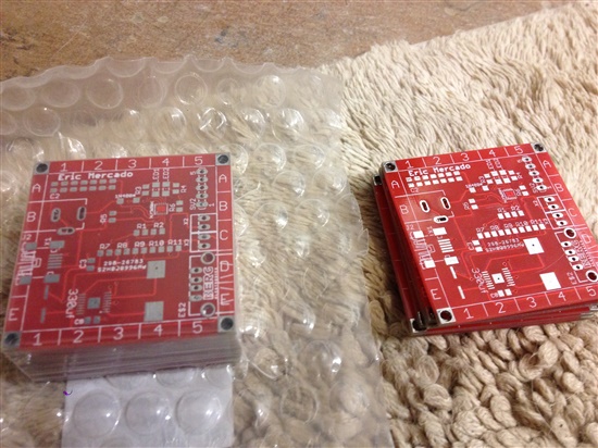
Here is a picture of the first prototype board. It worked but after i changed some values on the LBI it suddenly fried after plugging in a load on the 5V out. During normal operation before the chip fired the package was operating at room temperature. Coincidentally it got so hot when it fired, that the chip cleanly desoldered itself from the board. Haha i wish all bad chips did that!