Hi, everyone. I recently use a set of TI product for ultrasonic imaging. Here are several problem that I have met. Really Need your help T_T !
Q1: I have already read Mariusz’s post (http://e2e.ti.com/support/other_analog/imaging_afes/f/239/t/230591.aspx) about how to get two or more chips LM96570 synchronous in multichannel application. So I have the same doubt because I need to use four chip with my application.
Q2: There are so many supply voltages for LM96550 to make it work well. How to simplify this supply design? Take my design for example. And please let me know if there is any unreasonable point.
I use a power-supply module to supply +50V and -50V; then use LDO to generate +40V and -40V from +50V and -50V respectively; use LDO to generate +10V and -10V from input power supply +12V and -12V respectively; and input power supply +3.3V.(Power +12V, -12V, +3.3V, is external input power)
Q3: A serious problem, that the power supply pin called VDD/VSS is break through being shorted with GND, is occurred during our firstly use. Why? It confuses me.
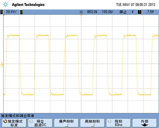
The schematic is showed as follow figure 1. The LM96550 is configured “CW” mode, so its output pulse is default 10MHz positive & negative high voltage pulse, as we measured in figure 2. When power on, this pulse is driving the LM96530. And the supply current grows high abnormally. Then we power it down immediately, and find that the power supply pin VDD/VSS have already been break through, shorted with GND.
It doesn’t make sense that the LM96530 is declared to accept the continuous wave up to +/- 60V in datasheet. But do NOT give the maximum acceptable frequency of continuous wave. So I guess that whether the frequency is too high that causes fatal damage to LM96530!!! Anyone can confirm my assumption.
Figure 1.
Figure 2.
Q4: LM96530 can be work well under single trigger. We find a fact that LM96530 can NOT be completely switched off. See figure 3, we input a high voltage pulse (the blue line indicated, almost -50V which is lasting 250ns) which results in some leakage peak (the yellow line indicated) at high voltage pulse edge location.
Figure 3.
Q5: Following Q4, we switch on one channel of LM96530. The output of LM96530 shows as figure 4, with a strong oscillation lasting about 5 us. When we put a 100nF cap between LM96530 output and GND close to LM96530, the result shows in figure 5. The effect is remarkable. So is it recommended to put such a cap at the each output of LM96530? But there is still an echo-like wave at rising edge, witch maybe wrongly regarded as front reflecting wave. Is there a way to eliminate it?
Figure 4.
Figure 5.
Q6: It’s sure that LM96511 is compatible with LM96530. But, if I replace LM96511 with AFE5805, is it still compatible with the output Vpp of LM96530. What’s the maximum analog input signal for AFE5805? In datasheet, it declares input voltage of LNA to be 250mVpp and internal diodes to be 600mVpp.
Thanks for your help !
SHIWEI


