Hello,
I require the source code for the MMB0 + ADS1299 EEF FE development board combo, specifically the firmware source code for the TMS230 DSP.
Many thanks!
Juan Sousa.
Hello,
I require the source code for the MMB0 + ADS1299 EEF FE development board combo, specifically the firmware source code for the TMS230 DSP.
Many thanks!
Juan Sousa.
A/D Converter: ADS1234-HT The RREG command: I need to issue the command to read out and poll DDRY bit status. Can I issue the command one time and keep reading out the register value to poll the DDRY bit status? Or I need to re-issue the command every time I read the same register and retrieve the DDRY status?
Hi ,
We performed Learning Cycle for bq27510-G3. We had done this before with G2. Based on one of the forums, we can reuse calibration values of the G2 for the G3 (they will be used in the same product).
We had proceeded with the learning cycle and generated the dfi. After generating the dfi, we had also "read" the the values to senc file (I2C).
Then using another Fuel Gauge, we programmed using the dfi but was shown, "Problem with the DFI".
During the Configure phase of the Characterization, we had encountered Error:Could not find subclass and offset for Gas Gauging.IT Cfg.Reserve Cap-mWh
based from this forum link: http://e2e.ti.com/support/power_management/battery_management/f/180/p/315386/1208546.aspx it is a bug of the bqeasy and we chould just proceed with the characterization.
In addition, during the update of the Golden Pack, an error popped us stating Error: Could not find subclass and offset for Gas Gauging.State.Cell0 Chg dod at EoC however, despite of this error popping, the software continued and generated the dfi file. So I had assumed that this is another bug in the software.
We are planning to conduct another learning cycle as soon as possible but we cannot proceed unless we had a solution to the error. Has anyone experienced the same thing with G3? How was this resolved?
Thanks,
Kat
ive been working out code to try and write a file system to an sd card using the file system from elmchan webite. i have example code from the LM3 microcntroller in order to port it. i think i've worked out most of the kinks, but im trying to set up my pins to associate them with the proper registers like the Tx and Rx, for ssi communication, and assigning them to port A pin 5 and pin 0 for example. but im getting an error code when i try to use:
IOCPinConfigPeriphOutput (uint32_t GPIO_A_BASE, uint8_t GPIO_PIN_5, uint32_t IOC_MUX_OUT_SEL_SSI0_TXD);
im putting this into my pinout function to set up my pin configuration. do i have to do an override or am i using the wrong function? if anyone has example code for a mu that is closer to the mu i am using, that would be appreciated
Hi,
As I read in the documentation, such as here http://www.ti.com/ww/en/launchpad/boosterpacks.html , boosterpacks seem to be stackable (i.e., i can put one on top of another).
Where can I find examples of it? Are there compatibility issues? I am specially interested in the combination of the sensor hub booster pack http://www.ti.com/tool/boostxl-senshub) + the sharp memory lcd booster pack (http://www.ti.com/tool/430boost-sharp96) with the TM4C123GXL board
Best
My name is Thomas Renick, and I need to figure out how to make Ethernet work on our tms570 micro-processor. I downloaded the lwip-1.4.1 file off of a TI forum and have been trying to get the tcpip portion of it to work, but its a whole lot of work. If anyone knows an easy way to get Ethernet to work using tcpip on a tms570 using code composer, I would greatly appreciate their help.
Thomas Renick
Hi,
Why is it that the SmartConfig generates two profiles one is with security type WPA and the other is with security type WEP. I assume that the WPA profile is my connection to my home wifi router.
Is it that the profile with security type WEP for Access Point mode?
I am using the httpserver as reference.
- kel
Hello,
I have already used the TI Webench Designer for a number of DC/DC voltage converter designs and have been generally pleased with the results. A few days ago I used the application again to see what it suggested for getting slightly more current out of a buck regulator design it had suggested before. To my surprise, the smallest footprint it could come up with was nearly twice as large. I got the same results even when I put in the original parameters I had used for the first design. It seems that the difference is that it is now only recommending electrolytic and tantalum caps and not MLCCs as it has done in the past. Does anyone know why this has changed? I understand that MLCCs have their issues, but they can still be significantly over specified and still be smaller than what is being recommended. Is there something newly discovered about MLCCs that I don't know that made TI change their mind as to their suitability?
Any advice would be much appreciated.
I have just tried the Blinky tutorial on my shiny new ccsv6 download. I get to the point where I click on the app.js and I get a Windows Script Host error. Line: 5, Char: 1, Error: Object expected, Code: 800A138F, Source: Microsoft JScript runtime error.
Anyone know of a reason why this is so?
Dear Support,
we use a F28M35H52C1 at the TMDSDOCKH52C1 Kit. At the moment we are developing a bootloader for our main application. For the M3 CPU we are a the point that we can programm our main application via the bootloader and jump to the main application. (The C28 CPU is ignored at the moment)
In the main application we get a FaultISR directly after FlashInit or in FlashGainPump function. Leave this part out via the debugger the rest of the application seems to work. (testet communication via Uart). Before leaving the bootloader we disabled the interrupts and called FlashLeavePump().
Programming the main appilcation via CCS (6.0.1.00040) everything runs fine as it should.
Info about Jump to the main application:
Setting the _c_int00 address:
		boot: load = 0x21a694
		{
			-l rtsv7M3_T_le_eabi.lib<boot.obj>(.text)
		}
Jump from the bootloader:
int main(void) {

...

  Main_SpringeZuHauptprogramm(0x21a694 + 1);
  return 0;
}


static void Main_SpringeZuHauptprogramm(unsigned long address) {
 __asm(" mov sp, r0\n"   // sp is now *address
   " bx r0\n" );     // jump to *address
}

Flashinit routine:
void FlashUserInit() {
Fapi_StatusType oReturnCheck;
DCSMUnlockZone1CSM (&Zone1KEY);
DCSMUnlockZone2CSM (&Zone2KEY);
memcpy(&RamfuncsRunStart, &RamfuncsLoadStart, (size_t)&RamfuncsLoadSize);
FlashInit();
FlashGainPump();
oReturnCheck = Fapi_initializeAPI(F021_CPU0_BASE_ADDRESS, 100);
if(oReturnCheck != Fapi_Status_Success) return; // TODO Fehlermeldung
oReturnCheck = Fapi_setActiveFlashBank(Fapi_FlashBank0);
if(oReturnCheck != Fapi_Status_Success) return; // TODO Fehlermeldung
}HWREG(SYSCTL_MWRALLOW) = 0xA5A5A5A5; SysCtlClockConfigSet(SYSCTL_USE_PLL | (SYSCTL_SPLLIMULT_M & 0xA) | SYSCTL_SYSDIV_1 | SYSCTL_M3SSDIV_1 | SYSCTL_XCLKDIV_4); and SysCtlPeripheralDisable(SYSCTL_PERIPH_WDOG1); SysCtlPeripheralDisable(SYSCTL_PERIPH_WDOG0); are called in the main init routine before FlashUserInit.
Since the the main application works without the bootoader, the malfunction must have something to with the bootloader.
Thanks for your help in advance
Mathias
Hello,
It appears from the UIA (target) side implementing a custom transport for different interfaces is rather straight forward. Is the same true for System Analyzer in Code Composer?
If it is, are there some docs I can be pointed towards? If not, are there docs on the binary file format System Analyzer uses so I could have another app receive the data and put it into something System Analyzer can display?
Thanks!
Hello,
I am interested in using the TMS320F28027F in conjunction with the DRV8301 to drive and control a BLDC motor. However, I need to add these IC's + the MOSFETs to a custom PCB that has certain size and weight restrictions.
So, does the TMS320F28027F come preprogrammed with instaspin such that as soon as I send in a single PWM input, it will convert it to the 3 pwm outputs that I'll be sending to the DRV8301, and then subsequently to the nFETs and the motor? Or, do I need to buy a breakout/programmer to accomplish this?
Thanks,
Aleksandar Zivkovic
If you have 4 devices connected to this hub, and you are only talking to one or two of them, will the others have idle conditions on their USB bus? The reason I ask, is I'd like to take advantage of the idle condition for disabling power to a few of the devices, should we not be talking to them. I know the protocol itself handles this sometimes, but wanted to make sure that I understood that correctly. thank you
Hi,
I was running some calculations on C6678 DSPs of KS II. But small data size, the result goes correctly. But I found that for some larger data, (which is still less than 32 MB), the results become NaN.
Do youhave any hints on that?
Thanks
Cheng
Hi,
I am using LMH6574 high-speed video mux in mux expansion mode. I use the shutdown line (SD) to select the mux chips. When I disable mux1 and enable mux2, I see a long (~500ns) exponential settling to the desired output voltage. Details follow.
Inputs to the mux
To test the mux, I feed DC voltages separated by 0.1V into the mux inputs. So the inputs to Mux1 are: 0.1, 0.2, 0.3, 0.4V, and the inputs to Mux2 are 0.5, 0.6, 0.7, 0.8V. These voltages come from a AA battery driving a resistive divider (16x 10 ohm resistors in series). At present, Mux3 and Mux4 are de-powered (they are disconnected from the supply voltages).
About the board, and project goals
The circuit is implemented as surface mount on a pcb, with 4 mux chips forming a 16:1 mux. I select the mux chips by using the shutdown (SD) line. I do not use the ~EN line. The mux output will eventually be digitized by a 12-bit ADC. Signals of interest are 0-2V, so bit noise is ~0.5 mV. Short-term goal is to digitize at 16MHz (to get 1 MHz sampling of each of the 16 mux input lines), with long-term goal of 32MHz digitization of a 32:1 mux. So I want settling times of <60ns, with <30ns as the long-term goal.
The mux gain is set to ~unity (as suggested in Fig. 29 of LMH6574 datasheet, I use: Rf = 1.5k and Rg is omitted, not accounting for loading by inactive muxes for now). The mux outputs are series-terminated in 50 ohms, and then read by a coax connected to the scope with 50-ohm termination (see Schematic below). So there is a 2:1 attenuation between mux input and scope measurement (measured Vout values are 0.05, 0.1, 0.15, 0.2V when mux1 is active, and 0.25, 0.3, 0.35, 0.4V when mux2 is active).
The problem
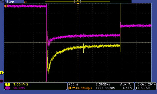
With two muxes powered, Vout shows a long (~500ns) exponential ramp following the transition from the first chip to the second (see Figure 1 below). No such ramp is seen on address changes within a chip, or at the selection of the first chip.
I have probed various places on the board, and do not see this waveform structure on the analog or digital grounds, or on the addressing lines (A0, A1), or on the SD line, or at the mux inputs. But I do see it on the output of the inactive mux (in this case Mux1) -- See Figure 2 below.
It appears that the inactive mux is driving Vout. I don't understand why that would be. Any help greatly appreciated.
Many thanks,
James
ps: I know from the data sheet that SD (not ~EN) should be used for mux expansion to prevent soft breakdown (when voltage between mux input and output exceed 2V). So I don't think soft-breakdown is to blame here since (1) as recommended I'm using SD (not ~EN), and (2) there is << 2 V between Vout and unused mux input (and we only see this exponential ramp immediately after the SD transition.
Figure 1
Yellow = Vout of mux pair, after the 50-ohm series termination of both mux chips. Notice exponential settling at the 5th step (the first step of Mux2). The Vout signal is transported from pcb to scope via 50-ohm BNC cable. Scope is terminated in 50 Ohms.

Figure 2
Yellow = Vout of mux (after 50 ohm series termination) seen via coax to scope terminated in 50 ohms.
Pink = output of the disabled mux (mux1, pin 13), probed between the mux and 50ohm series termination.
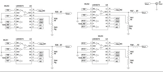
Mux Schematic:
Elapsed time capture is working well on the TM4C123G Launchpad, except for that the counter is not resetting after a capture event. I understand that this counter register reset is not automatic. From the datasheet page 715:
"After an event has been captured, the timer does not stop counting. It continues to count until the
TnEN bit is cleared."
So I inserted a command to clear the counter by using the TimerLoadSet command in the ISR, but the counter continues on where it left off after the capture event. Here is my complete code:
#include <stdint.h>
#include <stdbool.h>
#include "inc/tm4c123gh6pm.h"
#include "inc/hw_memmap.h"
#include "inc/hw_types.h"
#include "driverlib/sysctl.h"
#include "driverlib/interrupt.h"
#include "driverlib/gpio.h"
#include "driverlib/timer.h"
#include "driverlib/pin_map.h"

extern void WTimer0IntHandler(void);
uint32_t period_value;

int main(void)
{
	SysCtlClockSet(SYSCTL_SYSDIV_5|SYSCTL_USE_PLL|SYSCTL_XTAL_16MHZ|SYSCTL_OSC_MAIN); //40 MHz

	SysCtlPeripheralEnable(SYSCTL_PERIPH_GPIOF);
	GPIOPinTypeGPIOOutput(GPIO_PORTF_BASE, GPIO_PIN_1|GPIO_PIN_2|GPIO_PIN_3);
	SysCtlPeripheralEnable(SYSCTL_PERIPH_GPIOC);
	GPIOPinTypeTimer(GPIO_PORTC_BASE, GPIO_PIN_4);
	GPIOPinConfigure(GPIO_PC4_WT0CCP0);

	SysCtlPeripheralEnable(SYSCTL_PERIPH_WTIMER0);
	TimerConfigure(WTIMER0_BASE, TIMER_CFG_SPLIT_PAIR | TIMER_CFG_A_CAP_TIME_UP);
	TimerControlEvent(WTIMER0_BASE, TIMER_A, TIMER_EVENT_POS_EDGE);
	TimerIntEnable(WTIMER0_BASE, TIMER_CAPA_EVENT);
	TimerIntClear(WTIMER0_BASE, TIMER_CAPA_EVENT);
	IntEnable(INT_WTIMER0A);
	IntMasterEnable();
	TimerEnable(WTIMER0_BASE, TIMER_A);

	while(1)
	{
	}
}

void WTimer0IntHandler(void)
{
	TimerIntClear(WTIMER0_BASE, TIMER_CAPA_EVENT);
	period_value = TimerValueGet(WTIMER0_BASE, TIMER_A);
	TimerLoadSet(WTIMER0_BASE, TIMER_A,	0);
}
In a watch window I could see period_value increase after each capture, but the input at pin PC4 is a constant pulse width so period_value should likewise be constant. Likewise WTIMER0_TIMER_TAV also constantly increased after each capture event in the Memory Browser.
The TimerLoadSet description in the API page 549 says:
"This function configures the timer load value; if the timer is running then the value is immediately loaded into the timer."
So I should not have to stop the timer to reset it, yet it will not reset. Please advise.
I'm converting ~55V to 5V through a LM5116. When things start up, it can be presented with a very low load, perhaps 12-20mA. It seems that when this occurs that the device does not regulate very well, and goes under voltage.
when i put a bigger load on the device ( putting some 10R/10W resistors across the output ), the device operates normally.
Normal operation will se loads of between 0.2 an 2.5A on the device and in that range it seems to be ok. Its just at start up.
I'm sure i've read somewhere about not having enough load to make it work.

Hi everyone,
I found some conflicting information on the datasheet.
In table 9-1 it says that all GPIO only have burst request ability. In table 9-2 it says the opposite, which one is it?
Also, i take this advantage to ask one more thing, does the GPIO support DMA done interrupt?
I have +7.7V, -7.7V and analog ground.
I need +/- 15V referenced to the same analog ground. For a low noise analog application @ about 100mA.
Possible solution.
1. Boost DCDC with SYNC input creating an output of +/-15.5V or so. (I need help here)
2. Then a LDO filtering circuit. Planning on using TPS7A30 and TPS7A49 right now.
Do you have a circuit/part recommendation?
